A silicon compiler is a computer program that generates IC layouts from a high-level specification. In the SPIL silicon compiler a digital signal processing algorithm is specified in a language similar to Pascal, and IC layouts are generated using a simple register-transfer architecture with a data path controlled by a finite state machine. For a silicon compiler to be an effective design automation tool it is essential to include some type of performance evaluation to estimate power dissipation, layout area and propagation delays of the generated chip layout.
A design aid called EPAD is used for performance estimation of propagation delays, power dissipation and silicon areas of CMOS VLSI circuits. The objective is to provide the designer with an analysis of the IC layout. The designer can use this analysis to change the algorithm or intermediate levels of silicon compilation.
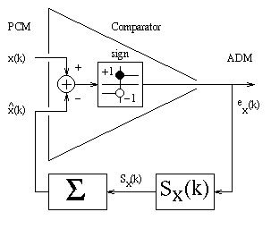
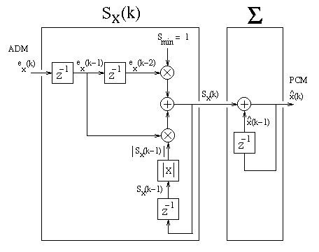
SPIL and EPAD are used in the design of a chip which compresses and decompresses speech by performing conversions between pulse code modulation and adaptive delta modulation. The algorithms for these conversions were written in the SPIL language, and layouts were generated and combined into one coder-decoder (codec) chip. An EPAD analysis was performed on this chip. Simulation files obtained from EPAD made it possible to identify possible design errors and to predict the maximum operating frequency. This was followed by fabrication and testing of the chip. Test results on fabricated chips compare favourably to EPAD predictions. The results made it possible to evaluate the effectiveness of the silicon compiler and to calibrate the performance evaluator.
The goal of this research is to show that the state of the art is advanced enough that a chip can be efficiently designed using SPIL with EPAD and that the chip can satisfy the requirements of specific applications.
PROGRAM PCM_to_ADM ;

CONST
   _data_width = 8 ;

VAR
    PCM_input  : input_port  CONNECT      DOWNWARD ;
    ADM_output : output_port CONNECT 0..0   UPWARD ;

    Ex      ,        { Starting from LSB(0) : Ex(k-1), Ex(k-2) }
    Sx_of_k ,                     { Step to next predicted PCM }
    X_of_k  : integer ;                      { Last PCM output }

PROCEDURE _reset ;             { Chip initialization procedure }
BEGIN
    Ex      := 0 ;                { Make Ex(k-1) = Ex(k-2) = 0 }
    X_of_k  := 0 ;
    Sx_of_k := 0 ;
END ;

BEGIN
   IF Sx_of_k < 0    THEN Sx_of_k := 0 - Sx_of_k ;

   IF Ex = ???????0B THEN Sx_of_k := 0 - Sx_of_k ;

   _add_in_1 := Sx_of_k ;          { IF Ex(k-2) = 1 THEN       }
   IF Ex = ??????1?B THEN          {                           }
      _add_in_2 :=  1              {    Sx_of_k := Sx_of_k + 1 }
   ELSE                            { ELSE                      }
      _add_in_2 := -1 ;            {    Sx_of_k := Sx_of_k - 1;}
   Sx_of_k := _add_out ;           { (No over/under-flow check)}

   X_of_k := X_of_k + Sx_of_k ;    {  No over/under-flow check }

   Ex := Ex << 1 ;   { Shift signals left   i.e. one time step }

   IF PCM_input > X_of_k THEN Ex := Ex + 1 ;

   ADM_output := Ex ;
END.         { PCM_input must have remained valid all the time }
PROGRAM ADM_to_PCM ;

CONST
   _data_width = 8 ;

VAR
    ADM_input  : input_port  CONNECT 0..0   UPWARD ;
    PCM_output : output_port CONNECT      DOWNWARD ;

    Ex      ,        { Starting from LSB(0) : Ex(k-1), Ex(k-2) }
    Sx_of_k ,                     { Step to next predicted PCM }
    X_of_k  : integer ;                      { Last PCM output }

PROCEDURE _reset ;             { Chip initialization procedure }
BEGIN
    Ex      := 0 ;                { Make Ex(k-1) = Ex(k-2) = 0 }
    X_of_k  := 0 ;
    Sx_of_k := 0 ;
END ;

BEGIN
   IF Sx_of_k < 0    THEN Sx_of_k := 0 - Sx_of_k ;

   IF Ex = ???????0B THEN Sx_of_k := 0 - Sx_of_k ;

   _add_in_1 := Sx_of_k ;          { IF Ex(k-2) = 1 THEN       }
   IF Ex = ??????1?B THEN          {                           }
      _add_in_2 :=  1              {    Sx_of_k := Sx_of_k + 1 }
   ELSE                            { ELSE                      }
      _add_in_2 := -1 ;            {    Sx_of_k := Sx_of_k - 1;}
   Sx_of_k := _add_out ;           { (No over/under-flow check)}

   X_of_k := X_of_k + Sx_of_k ;    {  No over/under-flow check }

   Ex := Ex << 1 ;   { Shift signals left   i.e. one time step }
   IF ADM_input = ???????1B THEN EX := Ex + 1 ;

   PCM_output := X_of_k ;
END.         { ADM_input must have remained valid all the time }
https://www.ece.unb.ca/petersen/pubs/theses/MASc/